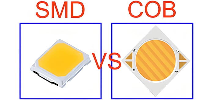
SMD vs. COB: Who Wins in LED Display Encapsulation?
Main differences between SMD and COB in the aspect of packaging technologies in LED displays include a way of encapsulation, size and weight, heat dissipation, maintenance and applications. The details are as follows:

1. Encapsulation method
SMD: the full name of Surface Mounted Device is a packaging technology that welds the packaged LED chip on the surface of the printed circuit board (PCB) through a precision mounting machine. This method requires the LED chip to be packaged in advance, form an independent component, and then affixed to the PCB.
COB: the full name of Chip on Board is a packaging technology that welds the bare chip directly on the PCB. It eliminates the packaging step of traditional LED lamp beads, directly sticks the bare chip to the PCB with conductive or thermal adhesive, and realizes electrical connection through metal wire.
2. Size and weight
SMD: although the component size is small, but limited by the package structure and pad needs, its size and weight are still limited.
COB: by eliminating the bottom pins and package housing, COB packages achieve extreme compactness, resulting in smaller and lighter packages.
3. Heat dissipation performance
SMD: mainly through pads and colloids for heat dissipation, heat dissipation area is relatively limited. Under high brightness and high load working conditions, heat may be concentrated in the chip area, affecting the life and stability of the display.
COB: the chip is welded directly to the PCB and can be cooled through the entire PCB board. This design significantly improves the heat dissipation performance of the display and reduces the failure rate due to overheating.
4. Maintenance convenience
SMD: because the components are mounted independently on the PCB, it is relatively easy to replace individual components during maintenance. This helps to reduce maintenance costs and shorten maintenance time.
COB: since the chip is welded directly to the PCB as a whole, it is not possible to remove or replace the chip separately. In the event of failure, the entire PCB board usually needs to be replaced or returned to the factory for repair, increasing the cost and maintenance difficulty.
5. Application Scenarios
SMD: because of its high maturity and low production cost, it is widely used in the market, especially in outdoor billboards, indoor TV walls and other projects that are cost sensitive and require high maintenance convenience.
COB: because of its high performance and high protection, it is more suitable for high-end indoor displays, public displays, monitoring rooms and other scenes with high display quality requirements and complex environments. For example, in the command center, studio, large dispatch center and other workers for a long time to watch the screen environment, COB packaging technology can provide a more delicate, uniform visual experience.
SMD and COB both have advantages in packaging technologies. With high maturity and a relatively lower cost of production in most projects, SMD technology found wide applications in the market, especially in projects that are sensitive to cost and convenient to maintain. Compared to it, so far, the COB packaging technology has some advantages of compact packaging, excellent heat dissipation effect, powerful protective performance, and so on. The COB is widely used in indoor display, public display and monitor rooms. Both of these two technologies will provide the user with more and more new options.


